5G Chip Testing: Small Environmental Test Chamber
Fifth-generation wireless technology demands semiconductor components that perform flawlessly under extreme environmental conditions, from sub-zero temperatures in outdoor base stations to tropical heat in dense urban deployments. A small environmental test chamber delivers the precise thermal and humidity control necessary to validate 5G chip reliability within compact laboratory footprints. These desktop testing solutions expose semiconductors to accelerated stress conditions that reveal design weaknesses, manufacturing defects, and long-term degradation patterns before commercial deployment. With 5G chipsets operating at millimeter-wave frequencies and generating significant heat loads, rigorous environmental validation ensures network infrastructure reliability across diverse global climates.
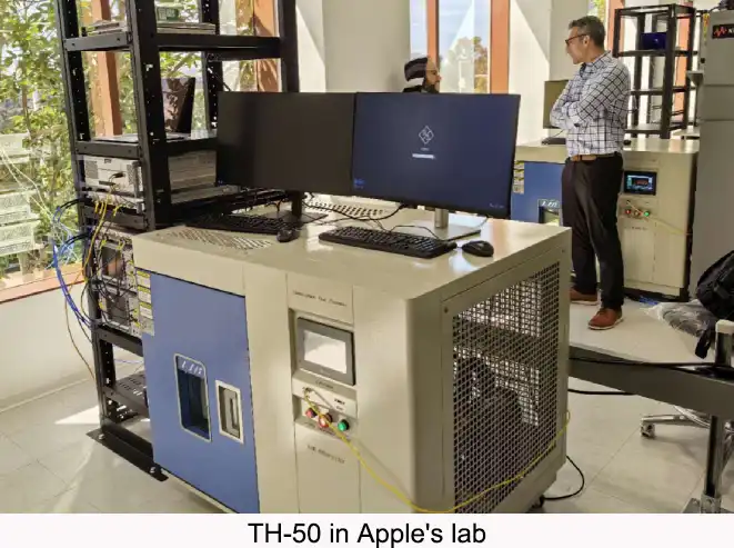
Why Is Environmental Testing Critical for 5G Chip Reliability?
High-Frequency Operation Thermal Challenges
5G semiconductors process signals at frequencies exceeding 28 GHz, generating substantially more heat than previous wireless generations. This thermal output concentrates in microscopic junction areas measuring mere nanometers, creating intense localized temperature gradients. Environmental chambers cycling between -40℃ and +150℃ reveal how these thermal stresses affect chip performance, signal integrity, and junction reliability. Power amplifiers, RF transceivers, and baseband processors each exhibit unique thermal sensitivities requiring individualized validation protocols to ensure stable operation across specification ranges.
Outdoor Infrastructure Deployment Requirements
Unlike consumer electronics protected within climate-controlled environments, 5G network equipment operates continuously in uncontrolled outdoor conditions. Base station electronics mounted on cell towers experience direct solar radiation, winter freezing, summer heat waves, and humidity fluctuations throughout daily and seasonal cycles. Comprehensive environmental testing replicates these harsh conditions, identifying components vulnerable to moisture ingress, thermal fatigue, or performance drift. Temperature humidity test chambers accelerate years of outdoor exposure into weeks of controlled testing, compressing development timelines while improving deployment reliability.
Supply Chain Quality Assurance Demands
Global semiconductor supply chains involve multiple fabrication facilities, assembly locations, and component suppliers. Environmental testing provides objective performance verification across these diverse manufacturing sources. Chambers maintaining ±0.5℃ temperature fluctuation and ±2.5% RH humidity deviation deliver the measurement precision necessary to detect subtle process variations between production batches. This quality assurance capability protects network operators from deploying equipment containing marginal components that might fail prematurely under operational stress, causing costly service interruptions.
Compact Test Chambers for Semiconductor Thermal Validation
Laboratory Space Optimization
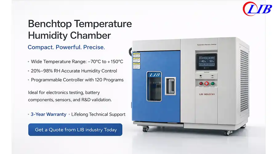
Semiconductor research facilities allocate valuable cleanroom and laboratory space to numerous specialized equipment systems. Traditional environmental chambers occupying several square meters create space allocation challenges in already-crowded facilities. Desktop testing solutions with 50L and 80L capacities fit comfortably on standard laboratory benches, positioning environmental validation capabilities directly adjacent to characterization equipment, probe stations, and analysis instrumentation. This spatial efficiency allows multiple testing stations within facilities previously accommodating only single large chambers.
Benchtop Accessibility Advantages
Engineers conducting iterative chip validation require immediate access to test samples throughout evaluation cycles. Walk-in chambers necessitate physical entry for sample manipulation, introducing cleanroom contamination risks and workflow interruptions. Small environmental test chambers place specimens at convenient working height with front-access doors enabling rapid sample exchange. The double-layer insulating glass observation window with built-in LED lighting permits continuous visual monitoring without opening the chamber, maintaining thermal stability during extended tests while allowing real-time defect observation.
Electrical Integration Simplicity
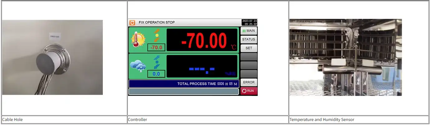
Semiconductor testing equipment demands substantial electrical infrastructure - dedicated circuits, voltage regulation, and sometimes three-phase power distribution. Compact environmental chambers operate from standard laboratory outlets (110V/220V), eliminating expensive electrical upgrades and infrastructure modifications. The 50mm cable port accommodates instrumentation wiring, power connections, and thermocouple leads without compromising chamber seal integrity. This plug-and-play convenience accelerates testing program implementation and simplifies chamber relocation when facility layouts evolve.
|
Chamber Feature |
TH-50 Model |
TH-80 Model |
Semiconductor Testing Benefit |
|
Internal Dimensions |
320×350×450 mm |
400×400×500 mm |
Accommodates PCB assemblies |
|
Temperature Range |
-40℃ to +150℃ |
-40℃ to +150℃ |
Full specification testing |
|
Humidity Control |
20% to 98% RH |
20% to 98% RH |
Moisture sensitivity validation |
|
Temperature Uniformity |
±2.0℃ deviation |
±2.0℃ deviation |
Consistent multi-site results |
|
Heating Rate |
3℃/min |
3℃/min |
Rapid thermal cycling |
|
Footprint |
820×1160×950 mm |
900×1210×1000 mm |
Benchtop compatible |
Temperature Cycling and Humidity Testing for 5G Components
Thermal Shock Resistance Evaluation
5G infrastructure equipment transitions rapidly between operational states - high-power transmission generating substantial heat followed by idle periods allowing cooling. These thermal transients create mechanical stress at material interfaces where components with different thermal expansion coefficients bond together. Rapid temperature cycling at 1℃/min cooling and 3℃/min heating rates replicates these operational transitions. Solder joints connecting chips to substrates experience repeated expansion-contraction cycles that eventually produce fatigue cracks. Testing chambers cycling between temperature extremes hundreds of times compress months of field operation into days of accelerated evaluation.
Moisture Sensitivity Level Classification
Semiconductor packages absorb atmospheric moisture through polymer molding compounds and substrate materials. When these moisture-saturated packages undergo high-temperature reflow soldering or operational heating, internal water vapor expands rapidly, creating delamination between die and package materials - a failure mechanism called "popcorning." Industry standards define Moisture Sensitivity Levels (MSL) through precise humidity exposure followed by thermal stress. Chambers maintaining 85℃ at 85% RH for specified durations classify components into MSL categories determining handling requirements throughout manufacturing and assembly processes.
Condensation and Dew Point Testing
Base station electronics operating in humid climates experience condensation when equipment surfaces cool below ambient dew points during overnight temperature drops. This moisture accumulation on powered circuit boards creates electrical leakage paths, corrosion initiation sites, and potential short circuits. Environmental chambers programmed for controlled condensation cycles expose 5G electronics to these conditions while monitoring electrical performance degradation. Conformal coatings, moisture barriers, and enclosure designs undergo validation ensuring protection against condensation-induced failures throughout anticipated service life.
How Do Environmental Chambers Support 5G Chip Performance Testing?

RF Performance Temperature Dependence
Millimeter-wave 5G signals exhibit extreme sensitivity to component temperature variations. Power amplifier gain, phase noise, and output power drift significantly across operating temperature ranges, directly impacting signal quality and transmission distance. Small environmental test chambers equipped with RF feed-through connectors enable continuous performance characterization while controlling device temperature precisely. Engineers map performance parameters across temperature ranges, developing compensation algorithms and identifying optimal operating windows. The PT100 Class A sensors with 0.001℃ resolution ensure measurement accuracy matching sophisticated RF test equipment precision requirements.
Junction Temperature Management
Semiconductor junction temperatures during operation often exceed ambient chamber temperatures by 50-100℃ due to self-heating from electrical power dissipation. Accurate reliability testing requires controlling junction temperature rather than ambient temperature alone. Advanced testing protocols combine environmental chamber ambient control with device power dissipation, using thermal modeling and embedded temperature sensors to achieve target junction temperatures. This approach replicates actual operational thermal stress more accurately than simple ambient temperature exposure, improving field performance prediction accuracy.
Built-In Instrumentation Integration
Modern 5G chip validation requires simultaneous environmental stress and electrical characterization. Environmental test chambers with Ethernet connectivity and programmable controllers integrate seamlessly with automated test equipment, data acquisition systems, and analysis software. Temperature and humidity profiles synchronize with electrical test sequences, enabling correlation between environmental conditions and performance parameters. The color LCD touchscreen controller programs complex test sequences with 120 programs containing 100 segments each, creating sophisticated validation protocols addressing multiple stress combinations without manual intervention.
|
Test Parameter |
Measurement Precision |
5G Validation Application |
Typical Test Duration |
|
Temperature Stability |
±0.5℃ fluctuation |
RF gain characterization |
4-8 hours per point |
|
Humidity Accuracy |
±2.5% RH deviation |
Package moisture absorption |
24-168 hours |
|
Thermal Cycling |
-40℃ to +125℃ |
Solder joint fatigue |
500-1000 cycles |
|
High Temperature Storage |
+150℃ sustained |
Accelerated aging |
1000+ hours |
|
Temperature Humidity Bias |
85℃/85% RH |
HAST screening |
96-264 hours |
Accelerated Stress Testing for High-Frequency Electronic Devices
Highly Accelerated Stress Test Protocols
HALT (Highly Accelerated Life Testing) methodologies push components beyond specification limits to identify fundamental failure mechanisms and design margins. Environmental chambers supporting HALT testing for 5G semiconductors must achieve temperature extremes (-70℃ to +150℃) with rapid transition rates. These aggressive thermal stresses reveal weaknesses that moderate testing might miss, including marginal design margins, process defects, and material incompatibilities. The SUS304 stainless steel interior construction withstands repeated thermal shocks without degradation, maintaining chamber integrity throughout thousands of extreme cycles.
Temperature Humidity Bias Testing
THB (Temperature Humidity Bias) testing applies electrical voltage to semiconductor devices while exposing them to elevated temperature and humidity combinations. This accelerated stress induces electrochemical migration, corrosion, and dielectric breakdown mechanisms affecting long-term reliability. Standard THB conditions (85℃/85% RH) with operational voltage applied for 1000+ hours compress decades of field operation into manageable test durations. Compact chambers accommodate multiple devices under test simultaneously, maximizing throughput while maintaining the uniform conditions critical for statistically valid reliability predictions.
Thermal Cycling Acceleration Factors
Coffin-Manson relationships quantify how thermal cycling frequency and temperature range affect failure acceleration. Environmental chambers with programmable cycling enable optimization of test conditions balancing acceleration factor against realistic failure mechanism activation. Cycling between -40℃ and +125℃ at maximum rate produces different failure modes than slower cycles across identical ranges. Engineers tune cycling parameters based on target failure mechanisms - solder fatigue, die attach degradation, or wire bond stress - ensuring accelerated testing predicts actual field failures rather than inducing artificial failure modes absent from real deployments.
Reliable Environmental Simulation for Advanced Semiconductor Applications
Multi-Zone Thermal Gradient Creation
5G radio frequency modules contain multiple semiconductor dies operating at different power levels and temperatures within shared packages. Accurate validation requires creating controlled thermal gradients rather than uniform chamber temperatures. Advanced testing configurations position localized heating elements alongside chamber environmental control, simulating operational thermal distributions. The micro-circulation airflow system in compact chambers maintains stable baseline conditions while localized heaters create realistic hotspots. This sophisticated approach reveals thermal interaction effects between adjacent components impossible to detect through uniform temperature testing.
Low-Noise Operation for Sensitive Measurements
Millimeter-wave RF measurements demand extremely low electromagnetic interference and mechanical vibration levels. Traditional environmental chambers with large compressors and circulation fans generate both electrical noise and vibration that compromise measurement accuracy. Small environmental test chambers incorporating whisper-quiet compressor technology operate below 65 dB, minimizing acoustic and mechanical disturbances. This quiet operation permits precision RF characterization concurrent with environmental stress, eliminating the measurement gaps and correlation difficulties inherent in sequential environmental exposure and performance testing approaches.
Contamination-Free Testing Environment
Semiconductor reliability testing extends across weeks or months of continuous chamber operation. During these extended periods, outgassing from interior materials can deposit contaminants on sensitive chip surfaces, altering electrical characteristics and potentially masking genuine failure mechanisms. The SUS304 stainless steel construction throughout the test volume eliminates polymer outgassing sources. Double-layer tempered glass windows with silicone rubber sealing prevent external contamination ingress while maintaining visibility. This contamination control ensures observed performance changes reflect actual device degradation rather than environmental artifacts.
Programmable Complex Environmental Profiles
Real-world 5G base station operation involves continuously varying environmental conditions - daily temperature cycles, seasonal humidity changes, intermittent precipitation, and solar heating effects. Static chamber conditions fail to replicate these dynamic stresses adequately. Programmable controllers executing 120-program sequences with 100 segments each create realistic environmental profiles. Morning temperature ramps, afternoon peak temperatures, evening cooling, and overnight condensation cycles all program into automated sequences. This sophisticated environmental simulation reveals failure mechanisms that steady-state testing overlooks, particularly those involving thermal expansion mismatches activated specifically during transition periods.
LIB Industry Offers Rapid Cycling and High Uniformity for Demanding 5G Chip Reliability Tests
 |
 |
|||
Advanced Refrigeration System Performance
Rapid thermal cycling essential for accelerated semiconductor testing requires robust cooling capacity delivering consistent performance throughout extended validation campaigns. LIB chambers incorporate French TECUMSEH compressor systems engineered specifically for continuous duty cycles. These industrial-grade refrigeration units maintain cooling rates of 1℃/min even after thousands of thermal cycles, unlike consumer-grade compressors that degrade rapidly under continuous stress. The mechanical compression refrigeration system achieves -70℃ minimum temperatures, accommodating the most demanding cryogenic testing protocols for next-generation semiconductors.
Precision Control System Architecture
Maintaining ±0.5℃ temperature fluctuation across chamber volumes requires sophisticated control algorithms balancing heating, cooling, and circulation systems. LIB's advanced PID (Proportional-Integral-Derivative) control continuously adjusts system parameters based on real-time sensor feedback from multiple PT100 Class A temperature sensors. This multi-point monitoring detects thermal gradients instantly, triggering corrective adjustments before temperature deviations exceed specification limits. The result is exceptional spatial and temporal uniformity critical for reproducible semiconductor characterization across multiple test locations and repeated experiments.
Comprehensive Safety Protection Systems
Unattended operation during extended reliability testing demands failsafe protection mechanisms preventing equipment damage and sample loss during fault conditions. LIB small environmental test chambers incorporate redundant safety systems including independent over-temperature protection operating separately from primary controllers. If control system failures allow temperature excursions, physical thermostatic switches interrupt power automatically. Additional protections monitor refrigerant pressure, water levels for humidity systems, electrical current draw, and ground fault conditions. These multiple independent safety layers ensure testing continues reliably while protecting valuable 5G semiconductor samples.
|
Safety Feature |
Protection Mechanism |
Failure Prevention |
|
Over-Temperature |
Independent physical cutoff |
Sample thermal damage |
|
Humidifier Dry-Combustion |
Water level monitoring |
Heating element failure |
|
Refrigerant High-Pressure |
Pressure relief and shutdown |
Compressor damage |
|
Over-Current |
Circuit breaker integration |
Electrical fire prevention |
|
Earth Leakage |
Ground fault detection |
Personnel shock hazard |
|
Water Shortage |
Low-level sensor |
Humidity system damage |
Turnkey Installation and Validation Support
Implementing environmental testing programs requires more than equipment delivery - comprehensive support ensures optimal performance from day one. LIB Industry provides complete turnkey solutions encompassing chamber selection, installation planning, calibration verification, and operator training. Experienced application engineers work directly with semiconductor teams to develop testing protocols matching specific 5G validation requirements. This consultative approach leverages LIB's 16+ years of environmental testing expertise, helping customers avoid common implementation pitfalls and accelerate program deployment timelines.
Custom Configuration Capabilities
5G technology evolves rapidly, with each successive release introducing new frequency bands, modulation schemes, and power requirements. Standard environmental chambers may not address emerging validation needs as technologies advance. LIB's engineering team specializes in custom chamber modifications addressing unique requirements - specialized sample fixtures, integrated instrumentation ports, modified temperature ranges, or hybrid environmental-mechanical testing capabilities. This customization expertise ensures testing equipment adapts to evolving 5G specifications rather than forcing test compromises with inflexible standard equipment.
Global Technical Support Network
Semiconductor development operates continuously across global time zones, requiring support availability matching 24/7 development schedules. LIB maintains worldwide technical assistance infrastructure providing immediate response regardless of customer location or time. Remote diagnostics via Ethernet-connected controllers enable rapid troubleshooting without dispatch delays. The comprehensive 3-year warranty with lifetime service support includes replacement unit provision if repairs prove impossible during warranty periods, ensuring minimal testing program disruptions from equipment downtime.
Conclusion
Environmental validation forms the cornerstone of reliable 5G semiconductor development, revealing performance limitations and failure mechanisms before network deployment. Compact desktop chambers deliver laboratory-grade environmental control without dedicated facility requirements, positioning precision testing capabilities directly within engineering workflows. From thermal cycling acceleration to moisture sensitivity classification, these versatile platforms address comprehensive 5G chip validation requirements. Advanced control systems, robust refrigeration, and comprehensive safety features ensure consistent performance throughout demanding test protocols, protecting substantial investments in next-generation wireless infrastructure development.
FAQ
What temperature range covers typical 5G chip operational specifications?
Most 5G semiconductors specify operation from -40℃ to +85℃ ambient temperature, though junction temperatures during operation reach significantly higher. Comprehensive validation testing extends beyond specification limits to -70℃ and +150℃, identifying design margins and revealing potential failure mechanisms under extreme conditions.
How long does standard 5G chip reliability testing require?
Temperature cycling typically involves 500-1000 cycles between temperature extremes, requiring 2-4 weeks depending on cycle duration. High Temperature Operating Life (HTOL) testing continues 1000+ hours at elevated temperatures. Complete qualification programs combining multiple test types span 2-3 months of continuous chamber operation.
Can small chambers accommodate multiple 5G devices simultaneously?
Absolutely. The 50L and 80L chamber volumes with adjustable SUS304 stainless steel shelving accommodate numerous semiconductor devices, evaluation boards, or packaged modules. Proper spacing ensures adequate airflow circulation maintaining temperature uniformity across all test positions, enabling parallel testing that maximizes throughput efficiency.
Advance Your 5G Semiconductor Testing with LIB Industry
As a trusted environmental test chamber manufacturer and supplier, LIB Industry delivers precision-engineered solutions optimized for semiconductor validation. Our application specialists provide expert guidance selecting chamber configurations matching your specific 5G testing requirements. Contact our technical team at ellen@lib-industry.com to discuss how our compact environmental chambers enhance your chip reliability programs.