Thermal Shock Resistance in Industrial Electronics: Testing Standards & Thermal Cycling Test Chambers
_1773978265968.jpg "blog-1-1") Thermal shock resistance tells us if industrial electronics can handle the sudden changes in temperature that happen in real-world settings, like when machines are cold-started or when power equipment quickly goes from no load to full load. Most of the time, this resistance is evaluated in either a thermal cycling test chamber or a specialized thermal shock system. These test environments expose parts to alternating temperature extremes, but with different transition speeds.
Thermal shock resistance tells us if industrial electronics can handle the sudden changes in temperature that happen in real-world settings, like when machines are cold-started or when power equipment quickly goes from no load to full load. Most of the time, this resistance is evaluated in either a thermal cycling test chamber or a specialized thermal shock system. These test environments expose parts to alternating temperature extremes, but with different transition speeds.
Components that pass strict thermal stress tests have much lower failure rates in the field. This helps manufacturers avoid expensive warranty claims and allows end users to reduce unexpected equipment downtime in mission-critical industrial settings where reliability cannot be compromised after deployment.
Difference Between Thermal Shock and Thermal Cycling Testing
Transition Speed as the Defining Variable
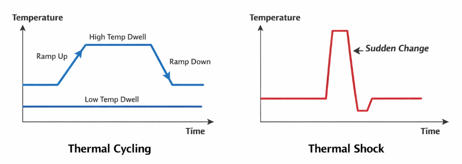
In thermal shock testing, a sample is moved quickly between hot and cold zones—often in less than a minute. This sudden change stresses materials much more than gradual variation. Thermal cycling, on the other hand, raises or lowers the temperature inside a chamber at rates that are usually between 5 and 15 degrees per minute. While this ramp speed is still rapid compared to ambient climate shifts, it provides a much softer thermal profile than a direct shock transfer.
Dual-Zone Versus Single-Chamber Equipment
Dual-zone or triple-zone equipment is often used for thermal shock testing. In these specialized systems, an automated basket transfers the object rapidly between physical hot and cold compartments. In contrast, an environmental thermal cycling chamber changes the air temperature inside a single closed workroom without moving the specimen itself. It relies on high-output refrigeration compressors and precision heating elements to transition the internal air volume dynamically.
Choosing the Right Method for a Given Component
Which method works best depends on how the components are packaged, because a sudden change in temperature can break sensitive glass-to-metal seals that would easily work fine under gradual cycling. When deciding whether shock, cycling, or both should be included in an approval plan, engineering teams evaluate governing industry standards and historical field failure data to build an accurate stress model.
How Rapid Temperature Changes Stress Electronic Components
Differential Expansion at Material Interfaces
When the temperature changes, each material joined inside an electronic structure—from the silicon die to the copper lead frames and epoxy encapsulant—grows and shrinks at its own rate based on its Coefficient of Thermal Expansion (CTE). When these temperature shifts happen quickly, adjacent materials do not expand uniformly, generating severe shear stress directly at bonded material interfaces.
Internal Versus Surface Temperature Lag
During fast temperature shifts, the exterior surface of a component adapts to the atmospheric environment sooner than its internal core. This thermal lag creates temporary internal temperature gradients. When this internal lag happens, it imposes extra mechanical stress on top of bulk material expansion, causing micro-structural fatigue to accumulate with each successive temperature wave.
Cumulative Fatigue Across Repeated Exposure
A single temperature transition rarely causes visible damage on its own. However, repeated thermal exposure builds up cumulative micro-strains in solder joints and bonded surfaces. This behavior mirrors mechanical metal fatigue caused by repetitive bending; micro-cracks form slowly and propagate silently over time until a complete electrical open circuit occurs.
| Testing Method | Transition Speed | Typical Stress Focus | |
| Thermal Shock | Seconds to under 1 minute | Brittle fracture, seal cracking, glass interface failure |  |
| Thermal Cycling | 5–15°C per minute | Solder joint fatigue, gradual delamination, trace wear |  |
Common Industrial Electronics Failures Caused by Thermal Stress
Solder Joint Fatigue and Cracking
Ball grid array (BGA) and surface-mount solder joints absorb continuous shear stress from CTE differences between the IC package and the printed circuit board (PCB) beneath it. Cracks typically initiate at the outer corner joints furthest from the package's neutral point, gradually spreading inward until intermittent or permanent electrical open circuits display during operation.
Connector and Housing Embrittlement
When exposed to extreme cold over and over again—especially at the lower bound of industrial temperature ranges—plastic socket housings and cable jacketing can lose elasticity. A structural chassis that flexes properly at room temperature may fracture under minor mechanical vibration or shock after exposure to repeated thermal cycles.
Sensor Drift and Calibration Loss
When temperature stress is applied repeatedly, precision sensors relying on stable internal reference elements can shift out of calibration, even without exhibiting visible physical damage. This subtle failure mode is easy to miss during visual checks, which is why functional post-test verification is a vital component of any qualification program alongside visual inspection.
Evaluating Material Stability Under Extreme Thermal Transitions
Polymer and Encapsulant Behavior
Conformal coatings and epoxy mold compounds shield internal circuitry from external threats, but prolonged cycling can induce micro-cracks or trigger interfacial delamination. The chemical formulation chosen during design directly dictates how many thermal transitions an encapsulant can endure before compromising its moisture and contaminant barrier capabilities.
Metal Fatigue in Lead Frames and Traces
Copper lead frames and circuit board traces gradually lose flexibility over time when repeatedly strained by thermal expansion. Utilizing stress-relieving bend patterns and reinforced trace geometries helps extend service life when exposed to continuous heat cycling.
Ceramic and Glass Seal Vulnerability
Parts that are hermetically sealed with glass-to-metal interfaces are especially at risk during sudden temperature changes because glass cannot tolerate as much mechanical strain as flexible metals before breaking. Components relying on these seals often undergo separate thermal shock testing alongside normal thermal cycling to ensure hermetic integrity at peak transition speeds.
Standards Governing Thermal Resistance Testing

JEDEC JESD22-A106 for Thermal Shock
JEDEC JESD22-A106 spells out standardized conditions for testing semiconductor devices under thermal shock conditions. It dictates dwell times, transfer speeds, and temperature limits across multiple test classes, giving manufacturers and buyers a unified benchmark to evaluate component endurance claims.
MIL-STD-883 Method 1011 for Defense Applications
Thermal shock testing for microelectronic devices used in defense and aerospace applications is governed by MIL-STD-883 Method 1011. This method requires significantly shorter transfer times and wider temperature extremes than standard commercial tests, demanding specialized equipment capable of fast transfer times and precise dwell time control.
IEC 60068-2-14 for General Electronic Equipment
IEC 60068-2-14 outlines change-of-temperature testing across a broader scope of electrical and industrial hardware. Covering both gradual ramp profiles and rapid temperature shifts, it serves as an adaptable baseline standard for industrial equipment manufacturers operating outside semiconductor-specific frameworks.
| Standard | Governing Scope | Notable Requirement |
| JEDEC JESD22-A106 | Semiconductor devices | Standardized transfer speed classes and dwell bounds |
| MIL-STD-883 Method 1011 | Aerospace & defense microelectronics | Extremely short transfer times and wide temperature bounds |
| IEC 60068-2-14 | General electronic equipment | Flexible test profiles covering both shock and cycling scenarios |
Design Strategies to Improve Thermal Durability
Stress-Relief Geometry in Board Layout: Avoiding sharp right-angle trace bends and implementing curved routing near component leads reduces stress concentration points where thermal fatigue usually strikes first. Advanced thermal modeling tools during early board layout help identify high-strain zones prior to physical testing.
Material Pairing to Minimize CTE Mismatch: Selecting substrates, encapsulants, and lead frames with closely matched Coefficient of Thermal Expansion values minimizes shear stress at all bonded interfaces during temperature swings.
Underfill and Mechanical Reinforcement: Applying underfill under ball grid array packages spreads mechanical stress evenly across the entire package footprint rather than concentrating forces on individual solder balls, significantly extending overall cycle life during environmental qualification testing.
Environmental Testing Infrastructure: LIB Industry Thermal Cycling Solutions-3-Year Warranty, Lifetime Service
 |
 |
 |
 |
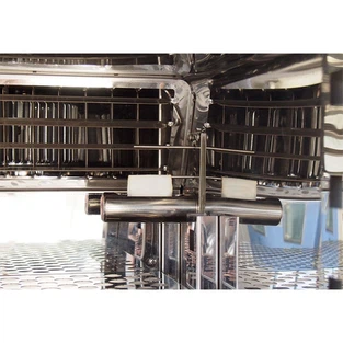 |
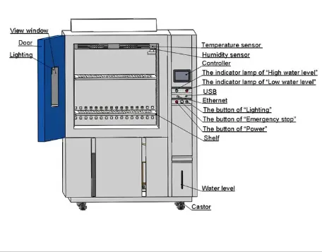
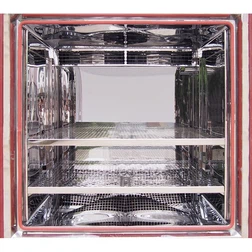
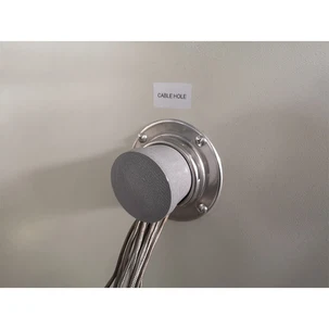
| Robust Workroom | Cable Hole | Temperature and Humidity Sensor |
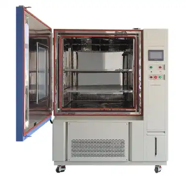
Executing reliable stress testing requires environmental chambers capable of strict compliance with international testing standards. LIB Industry provides specialized thermal cycling test chambers engineered specifically to meet the rigorous qualification demands of industrial electronics.
Precision Ramp Control: LIB Industry chambers feature programmable ramp rates from 5°C/min up to 15°C/min, utilizing ceramic-core nichrome heating elements and high-efficiency cascade cooling systems to maintain steady temperature variations within ±0.5°C.
Scalable Testing Capacities: From 100L benchtop chambers for individual IC qualification to 3000L walk-in rooms for complex industrial subassemblies, LIB Industry offers consistent environmental simulation capabilities across all production scales.
Turnkey Qualification Support: Beyond equipment manufacturing, LIB Industry delivers end-to-end laboratory support—including custom chamber design, installation, commissioning, operator training, and a comprehensive 3-year warranty backed by a global service network.
Conclusion
Industrial electronics engineered for challenging deployments differ from vulnerable designs by their ability to endure uncompromised thermal shifts. By utilizing a high-performance thermal cycling test chamber, distinguishing between shock and cycling parameters, recognizing critical failure mechanisms, and implementing standardized design mitigation strategies, manufacturers can guarantee long-term operational uptime and maintain product integrity across demanding industrial environments.
Frequently Asked Questions
In real-life applications, how does thermal shock testing differ from standard thermal cycling?
Using dual-zone equipment, thermal shock rapidly transfers specimens between extreme high and low temperature zones within seconds. Thermal cycling, on the other hand, raises and lowers air temperature inside a single work chamber at controlled ramp speeds (such as 5–15°C/min), applying a less immediate but highly effective fatigue stress.
How many thermal cycles are typically required for industrial electronic qualification?
Cycle counts depend on the target application standard and operating environment, typically ranging between several hundred to a few thousand repeats. High-reliability automotive and aerospace hardware requires significantly higher cycle counts than general commercial-grade industrial electronics.
Can thermal shock damage occur without showing obvious physical signs?
Yes. Internal solder joint micro-fissures, internal layer delamination, and sensor calibration drift frequently occur deep inside electronic components without displaying outward physical defects. This is why thorough qualification programs require both functional electrical verification and non-destructive inspection alongside visual checks.
Work With LIB Industry
Looking to upgrade your environmental testing facility or qualify new industrial hardware? As a specialized thermal cycling test chamber manufacturer, supplier, and turn-key factory partner, LIB Industry delivers custom environmental testing solutions from initial system design through installation and staff training.
Contact our technical team at ellen@lib-industry.com to explore equipment tailored to your industrial electronics thermal stress testing requirements.